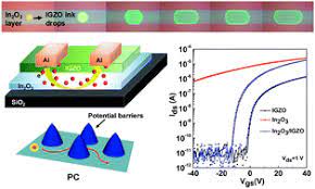
Semiconductor technology lies at the heart of modern electronics, driving innovation across a myriad of applications, from memory devices to flat-panel displays. Amorphous oxide semiconductors (AOSs) have emerged as promising candidates for next-generation storage devices and displays due to their unique properties. However, the performance of AOS-based thin film transistors (TFTs) has been hindered by contact issues, particularly high contact resistance at buried oxide-metal electrode interfaces. Addressing these challenges is crucial for unlocking the full potential of AOS technology. In a groundbreaking development, scientists at the Tokyo Institute of Technology have devised a novel method leveraging palladium-assisted hydrogen injection to enhance contact performance in AOS TFTs, paving the way for transformative advancements in semiconductor technology.
The Promise and Challenges of Amorphous Oxide Semiconductors:
AOSs have garnered significant attention for their potential applications in high-density memory devices and displays, owing to their high electron mobility, transparency, and low processing temperatures. However, the realization of AOS-based devices has been hampered by contact issues, particularly in vertically stacked architectures where buried oxide-metal electrode interfaces exhibit high contact resistance. This limitation compromises device performance, impeding advancements in storage density and energy efficiency.
Addressing Contact Issues with Palladium-Assisted Hydrogen Injection:
In a remarkable breakthrough, researchers at the Tokyo Institute of Technology have developed a pioneering method to alleviate contact issues in AOS TFTs using palladium-assisted hydrogen injection. This innovative approach involves utilizing palladium as a catalyst to dissociate hydrogen molecules and transport atomic hydrogen to deeply buried oxide-metal electrode interfaces within AOS devices. By facilitating the formation of a highly conductive oxide layer at the contact interface, palladium enables significant reductions in contact resistance and enhancements in charge carrier mobility.
Exploring the Mechanisms of Hydrogen Injection:
The success of the palladium-assisted hydrogen injection method hinges on the unique properties of palladium, which exhibits high hydrogen diffusion rates and solubility, even at low temperatures. By employing palladium thin film electrodes as hydrogen transport pathways, researchers were able to facilitate the rapid transport of atomic hydrogen to the oxide-metal interface, where it reacts with oxygen to form a conductive interfacial layer. This process effectively mitigates contact issues, leading to substantial improvements in device performance.
Experimental Validation and Performance Enhancements:
To validate the efficacy of the hydrogen injection method, researchers fabricated AOS TFTs with palladium electrodes and subjected them to heat treatment in a hydrogen atmosphere. The results were striking, with contact resistance reduced by two orders of magnitude and charge carrier mobility significantly enhanced. These improvements represent a significant leap forward in overcoming the inherent limitations of AOS-based devices, paving the way for their widespread adoption in next-generation memory technologies and displays.
Implications for Semiconductor Technology and Beyond:
The development of palladium-assisted hydrogen injection holds immense promise for revolutionizing semiconductor technology, offering a scalable solution to address contact issues in AOS-based devices. Beyond semiconductor applications, the versatility of this method opens up new possibilities for enhancing the performance of various electronic and optoelectronic devices. From high-density memory storage to advanced display technologies, the integration of palladium-assisted hydrogen injection promises to unlock new frontiers in electronics and drive innovations across diverse sectors.
The pioneering work conducted by researchers at the Tokyo Institute of Technology represents a significant milestone in semiconductor technology, offering a transformative solution to address contact issues in AOS-based devices. Through the strategic utilization of palladium-assisted hydrogen injection, researchers have successfully overcome barriers to device performance, paving the way for enhanced functionality, energy efficiency, and scalability in next-generation memory technologies and displays. As the semiconductor industry continues to evolve, the innovative methods developed by these researchers are poised to shape the future of electronics and drive advancements across a wide range of applications.
